DE10 Advance revC demo: Nios DDR4 SDRAM Test
From Terasic Wiki
Many applications use a high performance RAM, such as a DDR4 SDRAM, to provide temporary storage. In this demonstration hardware and software designs are provided to illustrate how to perform DDR4 memory access in QSYS. We describe how the Altera’s “Arria 10 External Memory Interfaces” IP is used to access the two DDR4-Sodimm on the FPGA board, and how the Nios II processor is used to read and write the SDRAM for hardware verification. The DDR4 SDRAM controller handles the complex aspects of using DDR4 SDRAM by initializing the memory devices, managing SDRAM banks, and keeping the devices refreshed at appropriate intervals.
Contents |
System Block Diagram
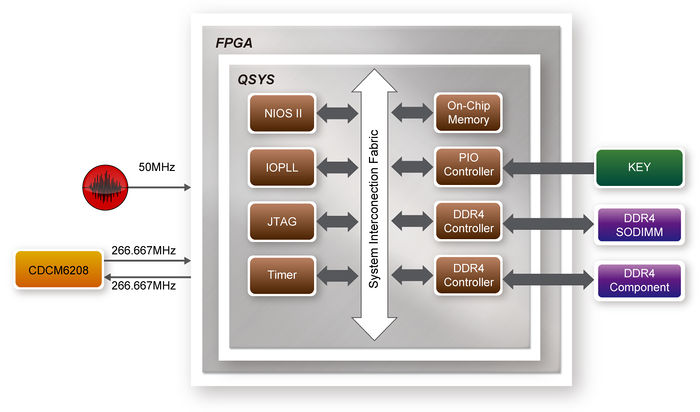
Figure 1-1 shows the system block diagram of this demonstration. The QSYS system requires one 50 MHz and two 266.667MHz clock source. The two 266.667 MHz clock source is provided by CDCM6208 clock generator on the board. The 50MHz is used by IO PLL to generate 200MHz for Nios Processor and On-chip Memory. The two 266.667MHz clock are used as reference clocks for the DDR4 controllers. There are two DDR4 Controllers are used in the demonstrations. Each controller is responsible for one DDR4 SDRAM. Each DDR4 controller is configured as a 1 GB DDR4-1066MHz controller. The DDR4A controllers are designed as 1GB rather 4GB is due to address space limitation of Nios II processor. Nios II processor is used to perform memory test. The Nios II program is running in the On-Chip Memory. A PIO Controller is used to monitor buttons status which is used to trigger starting memory testing.
- Figure 1-1 Block diagram of the DDR4 Basic Demonstration
The system flow is controlled by a Nios II program. First, the Nios II program writes test patterns into the whole 1 GB of SDRAM. Then, it calls Nios II system function (alt_dache_flush_all) to make sure all data has been written to SDRAM. Finally, it reads data from SDRAM for data verification. The program will show progress in JTAG-Terminal when writing/reading data to/from the SDRAM. When verification process is completed, the result is displayed in the JTAG-Terminal.
Design Tools
- Quartus Prime 18.0.0 Standard Edition
- Nios II Software Build Tools for Eclipse 18.0
Demonstration Source Code
- Quartus Project directory: NIOS_DDR4
- Nios II Eclipse: NIOS_DDR4 \software
- Nios II Project Compilation
Nios II Project Compilation
Before you attempt to compile the reference design under Nios II Eclipse, make sure the project is cleaned first by clicking ‘Clean’ from the ‘Project’ menu of Nios II Eclipse.
Demonstration Batch File
Demo Batch File Folder: NIOS_DDR4 \demo_batch
The demo batch file includes following files:
- Batch File for USB-Blaseter II: test.bat, test.sh
- FPGA Configure File: NIOS_DDR4.sof
- Nios II Program: DDR4_Test.elf
Demonstration Setup
Please follow below procedures to setup the demonstration.
- Make sure Quartus Prime and Nios II are installed on your PC.
- Make sure DDR4 SODIMM are installed on the FPGA board.
- Power on the FPGA board.
- Use USB Cable to connect PC and the FPGA board and install USB Blaster II driver if necessary.
- Execute the demo batch file “test.bat” under the folder “NIOS_DDR4\demo_batch”.
- After Nios II program is downloaded and executed successfully, a prompt message will be displayed in nios2-terminal.
- Press Key0~Key1 of the FPGA board to start SDRAM verify process. Press Key0 for continued test.
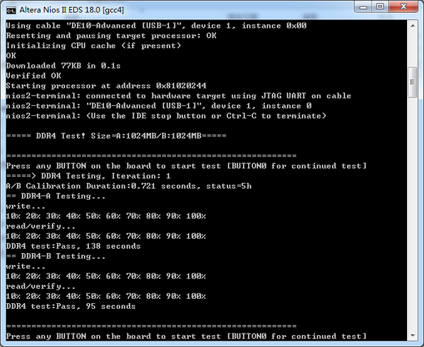
- The program will display progressing and result information, as shown in Figure 1-2.
- Figure 1-2 Progress and Result Information for the DDR4 Demonstration

