DE10 Advance revC demo: USB Type-C FX3 Loopback
From Terasic Wiki
USBC_FX3 RTL Demonstration Descriptions
This demonstration illustrates how the FX3 is working with the FPGA for USB3.0/USB2.0 data bulk in/out (data loop transmission). There is a USB type-C connector onto DE10-Advance board, a type-C cable is reversible for plugging in the USB type-C connector. This demonstration also implements the auto-switching mechanism for a type-C cable plugging in on either side.
- Function Block Diagram
Figure 2-1 Shows the function block diagram of the USBC_FX3 demonstration. This design comprises two parts, USB3.0/USB2.0 TX&RX crossbar switch controlling and FX3 data transferring. As the Type-C connector Is reversible, a Type-C port Controller (CYPD3125)is required for USB3.0/USB2.0 TX&RX crossbar switch controlling. When the Type-C cable is plugged in, the CC(Configuration Channel) signal is communicating with the controller. The controller then transfers the data to the Slave IC (FPGA) by I2C in Master mode, and There will be a salve I2C module in the FPGA to decode the signal and send the control signal to control the RX/TX direction of the PI3USB31532 USB3.0 signal. Here is a LED0 on the board to indicate the cable plugging direction, and LED1 indicates whether there is a USB connection signal or not. For the data transmission of FX3 module, FIFO and controller (implemented in the FPGA) combine FX3 module to perform the data bulk in/out loop. (For details, please refer to CYPRESS AN65974 Designing with the EZ-USB® FX3™ Slave FIFO Interface Chapter 11). All modules functions are described below:
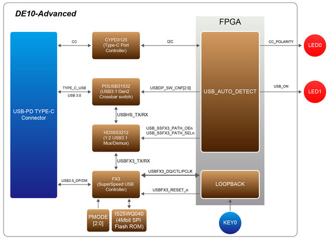
- Figure 2-1 Block diagram of the USBC FX3 design

USB_AUTO_DETECT: This module can decode the I2C signal from the Type-C Port Controller (CYPD3125 IC), then timely switch the RX/TX direction of Type-C port (by controlling the PI3USB31532 IC) and control the USB 3.0 Mux/Demux9 (HD3SS3212)switching to transfer the USB 3.0 signal to FX3 module. As shown in Figure 4-1, the LED0 indicates the Type-C connector RX/TX direction, the LED1 indicates the USB 3.0 signal input.
LOOPBACK: This module is designed as FX3 Slave FIFO Interface, the module combines the CYPRESS application(bulkloop.exe) to implement data bulk in/out loop demo.
KEY0: It is used to reset FX3 module.
PMODE[2:0]: The DE10-Advanced board has a 4Mbits Flash ROM, which can be used to program the FX3 firmware. This ROM is connected to FX3 through SPI interface. PMODE[2:0] is used to set the FX3 in program or boot status. The setting details is described in below steps.
The following are the descriptions of the platforms’ set up, as well as the test steps.
USBC_FX3 RTL Demonstration setup
- Hardware Setting Up
As shown in Figure 2-2:
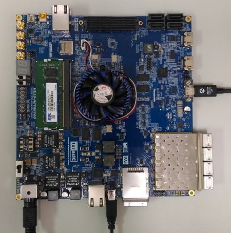
- Figure 2-2 USBC FX3 demo hardware setting up

- Design Tools
- Quartus Prime 18.0 Standard Edition
- Demonstration Source Code
- Quartus project directory: USBC_FX3
- Bitstream used: DE10_Advanced.sof
- Demonstration Batch File
- Demo batch file folder: demonstrations\USBC_FX3\demo_batch
- Demonstration Setup
- Connect the DE10_Advanced USB Blaster II connector (J20) to the host PC with a USB cable and install the USB-Blaster II driver if necessary.
- Use a Type-C cable to connect the DE10-Advanced and a PC (with a Type-C connector). As shown in Figure 2-3.
- Plug the 12V adapter to DE10_Advanced Board DC 12V power connector (J28).
- Power on the DE10_Advanced board.
- Execute the demo batch file “test.bat” from the directory \FPGA\USBC_FX3\demo_batch.
- Install the FX3 driver: The driver for Windows 7 is in the \FPGA\USBC_FX3\demo_batch\Driver\win7 folder, and the driver for Windows 10 is in the \FPGA\USBC_FX3\demo_batch\Driver\win10 folder.
- Use JP6, JP5, JP4 to set the PMODE[2:0] as “0F1” ( F indicates floating.
- Press KEY0 (RESET FX3 ).
- Re-plug the Type-C cable one time, Cypress Control Center will show Cypress FX3 USB StreamerExample Device and BOS (SuperSpeed Device capability), it indicates the USB3.0 Has completed the setup. When LED1 lights up, it indicates USB signal is detected. LED0 lights off indicates Type-C Cable two sides plugged with same directions, LED0 lights up indicates Type-C Cable two sides plugged with reverse directions.
- Execute the .exe application : \demo_batch\Host_app\loopback\bulkloop.exe , see Figure 4-4 below, press Start, you will see the Bytes Transferred IN/Out value increasing rapidly. For more information of bulkloop.exe, please refer to Cypress EZ-USB FX3 SDK Getting Started with FX3 SDK.
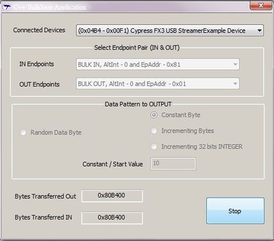
- Figure 2-3 FX3 bulk in out bulkloop

- Table 2-1 Summarizes the functional keys and details of each LED status.
- Table 2-1 The functional keys of the DE10-Advanced USBC_FX3 demonstration
- Table 2-1 Summarizes the functional keys and details of each LED status.
Name Description LED0 LED0 lights off indicates Type-C Cable two sides plugged with same directions.
LED0 lights up indicates Type-C Cable two sides plugged with reverse directions.
LED1 It lights up when the USB signal is detected.
- Program the FX3 firmware:(Optional)
- Execute the demo batch file “test.bat” from the directory \FPGA\USBC_FX3\demo_batch
- Execute Cypress Control: FPGA\USBC_FX3\demo_batch\Host_app\download_firmware\CyControl.exe
- Use JP6, JP5, JP4 to set the PMODE[2:0] as “F11”( F indicates floating).
- Press KEY0 (RESET FX3 ) , Cypress Control center will show Cypress FX3 USB Bootloader Device.
- Program software , In Control Center. Click Program FX3 SPI FLASH, as shown in Figure 2-4. Select file FPGA\USBC_FX3\demo_batch\FX3_Firmware\ SF_loopback.img . Wait until It reports “ Programming of SPI FLASH Succeeded”.
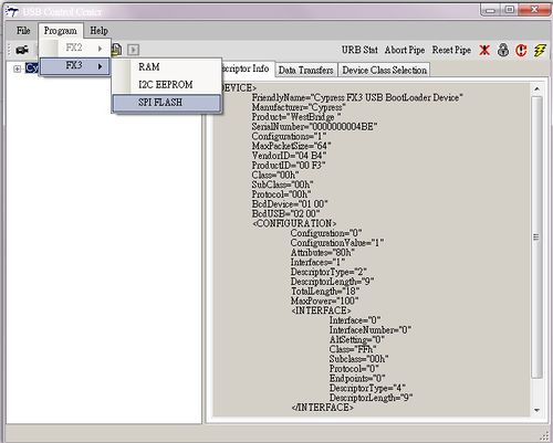
- Figure 2-4 Cypress Control Center
