Under Full HD resolutions (1920 x 1080), the HDMI connector is an integral part of the interface. Under 720p transmission, 1.485 Gb/s is needed to support uncompressed video and audio content. With HDMI, 24-bit audio and video can transfer at a speed of 165 Mpixels per second, with the bandwidth reaching up to 4 Gb/s. This not only meets the requirements for displaying 1080p, it also supports 192 kHz sampling which can transmit 8-track 24-bit audio signal. Under HDMI 1.3, transfer speeds were increased from the original 4.96 Gb/s to 10.2 GB/s, and color resolution was increased from 24-bit to 30-bit, 36-bit, and 48-bit (RGB or YCbCr), which results in an output capacity of more than 100 million colors. With the recent development of the HDMI 1.4a standard, 3D formats and even more features were added.
Under current progress of HDTV and HDMI specifications, simple image splitting has become quite a challenge on hardware design. In order to split images to reach Full HD standards, video processing core design is the focal point. This paper presents the design methodology for HDMI Full HD1080p video splitting, implemented on a DE3 FPGA platform in particular.
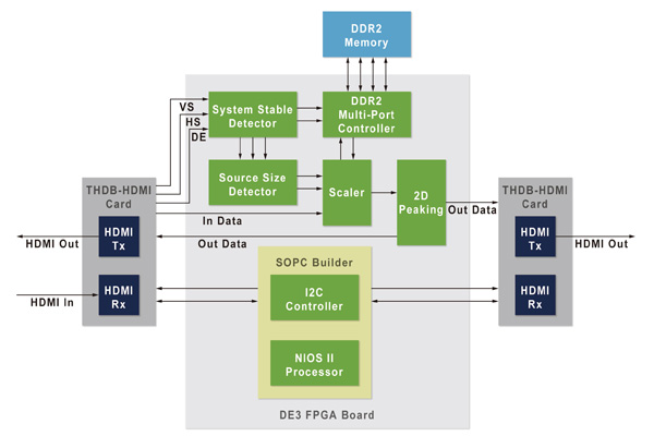
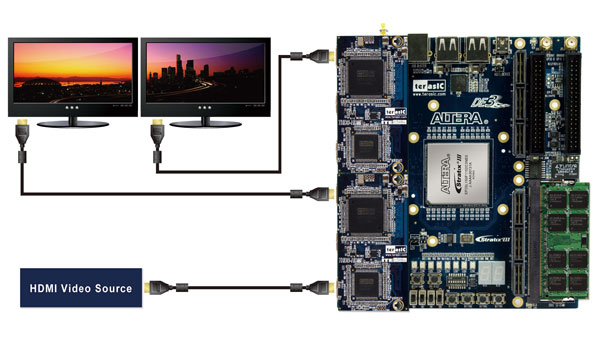
Figure 1 shows the basic HDMI Full HD1080p block diagram for video processing core design. The system receives an HDMI Full HD input, which after FPGA processing, is scaled vertically or horizontally according to the LCD screen. The image is then spanned across two (or four) 1920 x 1080 LCD screens. Figure 2 shows the actual setup of the DE3 FPGA hardware platform along with an HDMI daughter card for input/output which meets the requirements of HDMI 1.3.

Figure 1 < HDMI Full HD1080p split-screen block diagram >

Figure 2 < HDMI input/output using DE3 FPGA development platform and daughter card under HDMI 1.3 >
The system is composed of three portions:
(1) HDMI input/output settings controller core;
(2) HDMI control signal generator;
(3) HDMI video streaming processing core.
For the first portion, in HDMI input/output settings, controller core is established via the SOPC Builder in Figure 1. It is built with a combination of the Nios Processor and I2C Controller, which are in charge of setting and controlling HDMI input/output. The second portion is the HDMI control signal generator, which is composed of the System Stable Detector, Source Size Detector, and DDR2 Multi-port Controller in Figure 1. The System Stable Detector is in charge of automatically detecting switching between different resolution sources, so that the whole system can reset to match. Source resolution counter is responsible for scaling the image, frame size, and position according to the ratio of the front-end and back-end display.
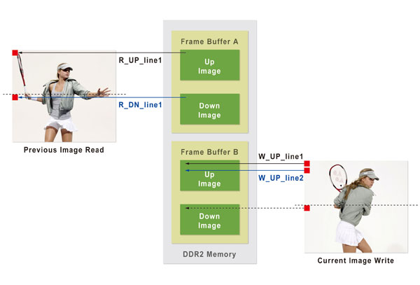
The DDR2 multi-port Controller is responsible for controlling the horizontal-splitting registers. The DDR2 memory is set up as ping-pong buffer structure (Figure 3 is an example of splitting one image into two), utilizing two identical frame storage devices. One frame is written, and another frame is read, which prevents flickering and tearing. If the horizontal is split from one frame to two, the DDR2 multi-port controller must split the operations into read and subsequently write. During the writing stage, two starting positions must be identified, one for the top half of the image, and the other for the bottom half of the image, simplifying the read portion of the DDR2 controller architecture. In the design, the read timings for the ports are equally allocated. As can be seen in Figure 3, one line is read, and when one line is written, only the top line is read at the read port. When the second line is written, then the first line of the bottom half is read.
As such, the DDR2 bandwidth is allocated for best performance, where the DDR2 can operate easily at 200 Hz with a 148.5 MHz Full HD input source, and hence there is no limit to vertical splitting.
The third portion of the HDMI video streaming processor core is made up of the scaler and 2D peaking. The scaler is responsible for adjusting the source information to the correct output size, either by linear or nonlinear amplification. During interpolation, the more reference points there are, the better quality of resulting image forms. It’s better to at least use bi-cubic interpolation. If edge-adaptive interpolation can also be considered, the high frequency portions of the image will be much clearer. 2D peaking is responsible for increasing the sharpness of the video, as after scaling operations, edges appear blurry. It's important to note that if scaling is not performed properly, artifacts such as halos and jags may appear after 2D peaking operation.
The experimental platform is shown in Figure 2, with the DE3 FPGA development kit handling all the functions of receiving and transmitting HDMI. The Sony Playstation 3 is the input HDMI source, generating a 1920 x 1080 Full HD progressive signal. The FPGA takes the source file and partitions it into two images, where it displays them on two separate HDMI monitors. Utilizing the Altera Stratix III 340 kit, with 340,000 logic elements, the experimental platform ran at 148.5 MHz, with the on-board DDR2 running at 200 MHz.

Figure 3 < The DDR2 memory forms a ping-pong buffer architecture on the DE3 platform – vertical splitting >
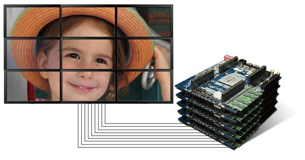
With the above mentioned design methodology, multiple frames (2x2, 2x3, 3x3, 3x4, etc.) can be formed with Full HD. Taking advantage of the re-stackable and modifiable nature of the DE3 platform , any hardware development kit is possible. Figure 4 displays the stacked DE3s and HDMI daughter cards which forms a 3 x 3 Full HD HDMI frame split processor. This is suitable for TV Wall applications.

Figure 4 < Stacked DE3 platforms and HDMI daughter card design–nine frames outputted through a video controller wafer >
This paper introduces the design of HDMI Full HD 1080p splitting processor core techniques in detail. It also describes how to use the DE3 FPGA development kit with THDB-HDMI daughter card to realize an HDMI system block. For more information on this subject, please visit hdmi.terasic.com
