Nowadays the whole world is working on high-end multi-layer PCB designs that operate at more than 10Gb/s, with the integration of high-speed circuitry analysis, theories and simulation technique experiences. Thus, American or European companies dominate in such markets. Few Asian companies have the resources to compete with American and European competitors in this niche market. Going along with TSMC, UMC and other large wafer manufacturers that are experiencing rapid breakthroughs in FPGA development, with 90nm quickly shrank all the way down to 28nm, and IO speeds gaining from 10Gb/s up to 30 Gb/s, the market demand for precise FPGA hardware and PCB design is likewise rapidly accelerating.
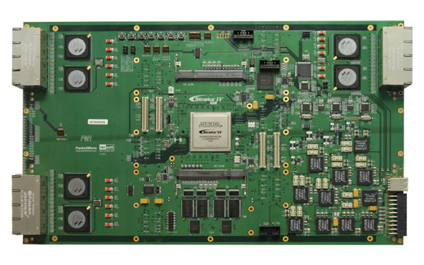
Figure 1 Terasic Technologies developed top-tier 40 nm Stratix IV FPGA for U.S.A. aerospace
In 2005, Altera’s newest FPGA system designs and manufacturing were transferred to Terasic Technologies. In the mid-2009, Terasic Technologies developed high-end 40nm Stratix IV FPGA system and PCB simulations for the leader in the U.S. aerospace industry. Presently, the system has already passed all function tests with flying colors. Figure 1 shows the system exterior with a 22-layer PCB. The measurements are 38.2 cm x 23.3 cm. This system became the pinnacle aerospace platform for research and applications projects. This article describes in detail the development process and the difficulties in PCB design.
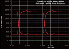
Figure 2 DDR3 Memory Simulation Results
When developing high-speed systems for FPGAs that are 40nm or under, developers must overcome numerous obstacles and use a variety of simulation tools, including SPICE, to solve high-speed circuit designs which face signal integrity problems. Through the analysis of concrete problems, developers must optimize components and make certain tradeoffs, such as layer architecture, dielectric materials, cable topology, cable length, cable width, and impedance matching components. Most of the signal integrity problems must be solved during the design phase based on the results of simulation. Figure 2 shows our simulation analysis of how impedance matching components affect the DDR3 ground signals. Through simulation, we can see how the use of termination matching resistor results in the least overshoot and undershoot of a signal.
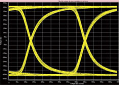
Figure 3 Eye Diagram Result
Through-hole Loss
Via loss depends on the unique characteristics of the through-hole, including size and shape of the pad, through hole length (through hole or blind via), stub, wiring layers, etc. These will all affect signal loss.
Ways to minimizing loss from through holes include not using pads and using bigger anti-pads to reduce parasitic capacitance effects; transmission routing should be on the exterior layers. Otherwise, using blind vias or back drills will lessen stubs and signal reflection. If ground-return vias are provided and closed to the signal vias by which high-speed signals travel from layer to layer in a PCB, the return current can also travel from one plane to another smoothly. Figure 4 illustrates the Via Stub Effect, which results from a signal going from top layer to inner layer via.
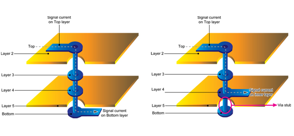
Figure 4 Via Stub Effect
SMT Pad Loss
The most common components in an FPGA multi-gigabit transmitter design are DC blocking capacitors, high-speed connectors, and PCI Express edge connectors. When differential signals trace any of these components into the SMT pad, the copper SMT pad width will be wider the differential signal traces. Width mismatch will result in impedance differences. Narrow paths will have higher impedance. Wider SMT pads will have lower impedance. In order to match impedance, we must think of other ways to align the SMT pad resistance.
Factors that affect the resistance, in addition to the line width and distance between the wire layer and copper reference layer, include dielectric permittivity and the thickness of copper in the wiring layer. Once the PCB structure is set, we can only change the distance between the wired layer and copper reference layer. We will try to make the wired layer reference the second copper layer, as if to increase the dielectric layer between the trace and copper, which makes the resistance increase. Thus, we can remove the first copper layer under the SMT pad to increase its resistance, and finally match the impedance of the trace width. Figure 5 illustrates the actual layout.
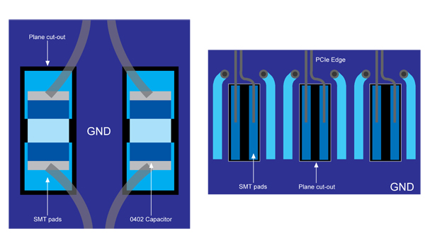
Figure 5 Changing layout and impedance
The above-mentioned PCB architectures all help realize high-speed transmission. In order to fully realize them, models must be established, simulated, and analyzed to control signal integrity. Through the design methods, we can achieve the right complicated systems and PCB designs at the first time. We can avoid the dilemma of retrying trial-and-error PCB designs that happened in the past.
