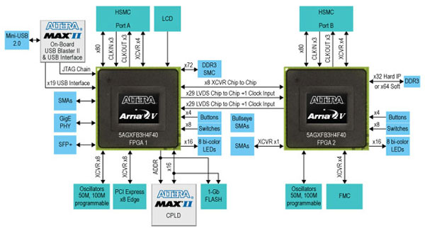
Altera Arria V GX FPGA Development Kit
Unit 1: Arria V GX FPGA: 5AGXFB3H4F40C5NES
- Memory
- 1,152-MB x72 DDR3 SDRAM
- 4.5-MB (1 Mb x 36) QDR II+ SRAM
- 1-Gb sync flash (x16)
- Communication ports
- PCI Express®
(PCIe®
) x8 edge connector
- HSMC Port A (four transceiver channels)
- USB 2.0
- Gbps Ethernet
- Chip-to-chip bridge with 29 LVDS inputs and 29 LVDS outputs, and x8 transceivers
- One SFP+ channel
- Bullseye connector (x1 channel)
- SMA connectors (x1 channel)
- Configuration
- JTAG
- Fast passive parallel (FPP) parallel flash loader (PFL)
- Buttons, switches, LEDs, and displays
- One reset configuration push button
- One CPU reset push button
- Three user push buttons
- Two configuration push buttons
- Eight dual in-line package (DIP) switches
- 16 user LEDs (eight bi-color diodes)
- 16x2 character LCD
Unit 2: Arria V GX FPGA: 5AGXFB3H4F40C5NES
- Memory
- x64 DDR3 SDRAM soft controller (or x32 hard intellectual property (IP) controller)
- Communication ports
- HSMC Port B (four transceiver channels)
- FMC Port (four transceiver channels)
- Chip-to-chip bridge with 29 LVDS inputs and 29 LVDS outputs, and x8 transceivers
- One serial digital interface (SDI) channel
- Bullseye connector (one transceiver channel)
- SMA connector (one transceiver channel)
- Configuration
- Buttons, switches, LEDs, and displays
- One CPU reset push button
- Three user push buttons
- Eight DIP switches
- 16 user LEDs (eight bi-color diodes)
Miscellaneous
- EPM2210GF324 system controller
- EPM570GM100 on-board USB-Blaster™
II download cable
Clocking
- 50-MHz oscillator
- 100-MHz and 125-MHz programmable oscillators
- SMA input (LVPECL)
Power
- Laptop DC input
- PCIe edge connector
System monitoring
- Power (voltage, current, and wattage)—per unit per rail
- Temperature (per FPGA die, local board)
Arria V GX FPGA Development Board Block Diagram