Altera 100G Development Kit, Stratix V GX Edition
Stratix V GX development board
- Featured device: 5SGXEA7N2F45C2N
- EPM2210F324C3N, MAX®
II 324-pin CPLD
FPGA configuration
- Fast Passive Parallel (FPP) configuration
- 1-Gb flash storage for two configuration images (factory and user)
- On-board USB-Blaster™ II cable for use with the Quartus® II Programmer, Nios® II software and System Console
- JTAG header for external USB-Blaster cable
Memory
- Twelve 2-Gb DDR3 SDRAM
- Two 72-Mb QDR II SRAM
General user input/output
- Four user push buttons
- Two DIP switches
- Eight user LEDs
- Two-line character LCD
- Ten configuration status LEDs
Components and interfaces
- 10/100/1000 Ethernet PHY and RJ-45 jack
- 48 transceiver channels
- Two channels for SMA interface
- Four channels for SFP+ interface
- Eight channels for QSFP interface
- 10 channels for CFP interface
- 24 channels for Interlaken interface
Temperature measurement circuitry
Power
- 19-V DC input
- 2.5-mm barrel jack for DC power input
- On/off power slide switch
- On-board power measurement circuitry
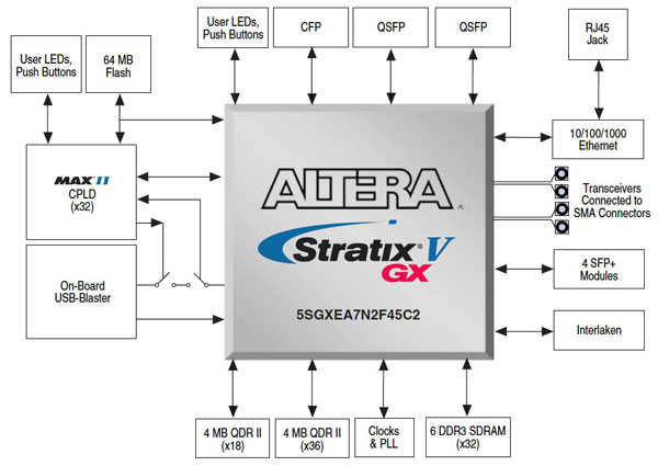
Altera 100G Development Kit, Stratix V GX Edition Block Diagram


