Altera Arria V GX Starter Kit
FPGA:
- Arria V GX 5AGXFB3H4F35C4N
System controller: MAX®
V 5M2210ZF256C4N
- Power monitor GUI
- Single analog-to-digital converter (ADC), eight channels
- Non-isolated power rail
- Fast passive parallel (FPP) x16 mode through parallel flash loader (PFL)
- Control and status registers
Embedded USB-BlasterTM
II:
HDMI 1.3 TX
- x4 XCVR, 2.7 Gbps (max by level shifter) and 270 MHz TX clock HDMI TX connector
- STMicroelectronics HDMI level shifter STHDLS101T
- Level shift XCVR PCML 1.5V <-> TMDS level
- DDC and HPD <-> HDMI compliant level
- Data channel up to 2.7 Gbps; HDMI 1.3 compliant
- Clock channel up to 270 MHz; enough to support 2.7 Gbps data rate
- HDMI specification: clock period = 10x of UI
SDI 3G
- x1 XCVR TX/RX loopback
- x2 SMB connectors and cable (cable not included in kit)
- Up to 2.97 Gbps
- Uses National Semiconductor driver/receiver LMH0384SQ/LMH0303SQx
- Requires 148.5 MHz and 148.35 MHz at XCVR refclk to support US and EU standard respectively
- Use VCXO to fine tune and lock to the recovered CDR frequency
HSMC
- x8 XCVR up to 6.375 Gbps
- Not complied to PCI Express®
(PCIe®
) HIP pin assignment
- x4 CMOS
- x8 TX and x9 RX differential interface using dedicated TX/RX channels
- x2 low-voltage differential signalling (LVDS) clock in
- x2 differential clock out
- I2C
- JTAG
- Minimum current support
- 2A @ 3.3V
- 1A @ 12V
- Dedicated clock domain from Si 5338 clock generator for xcvr refclk
- HSMC loopback with BTS GUI
SMA
- 1x XCVR TX/RX channel
- 1x LVPECL clock input
- 1X LVPECL clock output
Clocking
- Dedicated clock domain from Si 5338 clock generator for xcvr refclk
DDR3 SDRAM x32
- Micron MT41J64M16LA-15E DDR3 SDRAM 8MX16X8
- Two devices: 2 x16 width = x32
- BTS DDR3 SDRAM GUI using Uniphy and high performance (HP) controller II
SSRAM
- 512k x36, 18 Mb ISSI IS61VPS51236A
- Shared address or data with flash
User IO
- LCD character
- x4 DIP switch
- x3 PB
- x4 LED
Configuration
- FPP x16 mode
- Dual flash 512Mbit Numonyx PC28F512P30BF (52 MHz FMAX
)
- JTAG header
Embedded USB Blaster II
- Cypress Microcontroller CY7C68013A as USB PHY 2.0
- MAX II
Ethernet
- 10/100/1000 Base-T
- RJ-45 connector, on-board LED for link status
- Marvell Ethernet PHY 88E1111
- Requires 50 MHz clock from CLKIN
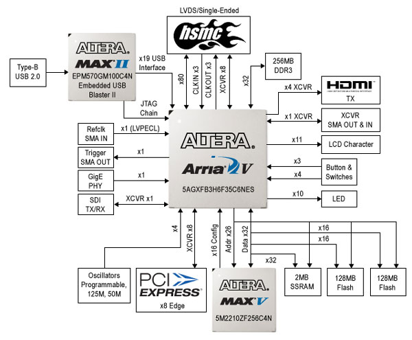
Altera Arria V GX Starter Board Block Diagram


