Altera Stratix IV GX FPGA Development Kit
Featured devices
- Stratix IV GX EP4SGX230KF40C2N FPGA or,
- Stratix IV GX EP4SGX530KH40C2N FPGA
Configuration status and set-up elements
- Fast passive parallel (FPP) configuration via a MAX®
II EPM2210 CPLD and flash memory
- On-board USB-BlasterTM
download cable using Quartus II Programmer
Clocks
- On-board clock oscillators: 50 MHz, 100 MHz, 125 MHz, 148.5 MHz, 155.52 MHz, and 156.25 MHz
- SMA connectors for external clock input
- SMA connectors for clock output
General user input/output
- LEDs
- LCD display
- Push-button and dual in-line package (DIP) switches
Memory devices
- 512-MB DDR3 SDRAM with a 64-bit data bus
- 128-MB DDR3 SDRAM with a 16-bit data bus
- Two 4-MB QDR II+ SRAMs with 18-bit data buses
- 64-MB sync flash and 2-MB SSRAM
Component and interfaces
- PCI Express x8 edge connector
- 10/100/1000BASE-T Ethernet PHY with RJ-45 connector
- Two HSMC connectors
- HDMI video output
- 3G-SDI video input and output
- Power measurement circuitry
- Temperature measurement circuitry
Power
- Laptop DC input
- PCI Express edge connector power
- Power measurement circuitry
Other features
- PCI Express half-length, full-height (6.6" x 4.376") board format
- RoHS compliant
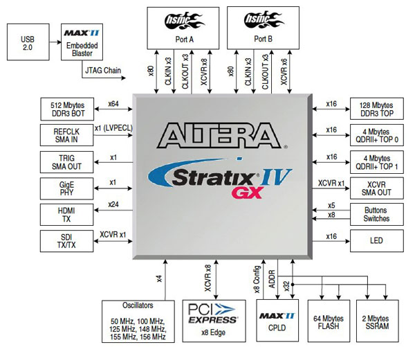
Altera Stratix IV GX FPGA Development Kit Block Diagram


