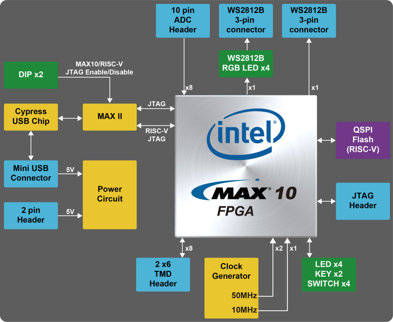
FPGA Device
- MAX 10 10M50DAF484C7G Device
- Integrated dual ADCs, each ADC supports 1 dedicated analog input and 8 dual function pins
- 50K programmable logic elements
- 1,638 Kbit M9K Memory
- 5,888 Kbits user flash memory
- 144 18 × 18 Multiplier
- 4 PLLs
User Interface
- Button x2
- Dip Switch x4
- Green LED x4
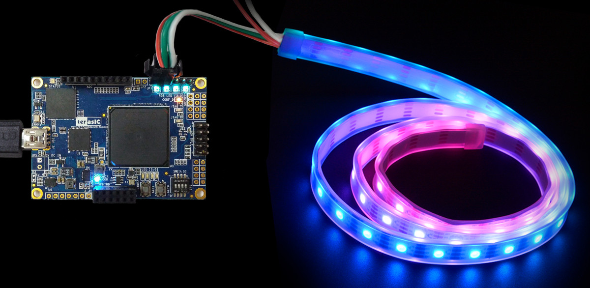
- RGB LED x4
JTAG
- On-board USB-Blaster II for programming MAX10
- On-board USB-Blaster II for programming RISC-V
- JTAG Master for programming the FPGA on other Boards.
Clock and Memory Devices
- Two 50 MHz single-ended, external oscillator clock source
- One 10 MHz single-ended, external oscillator clock source
- 64Mb QSPI Flash (Store RISC-V Code)
Expansion Connector
- 2x6 TMD Expansion Header
- 1x10 ADC Header
- Two 1x3 RGB LED Expansion header
Power Supply
- USB Type mini-AB port (5V)
- 2-pin external power header (4.4-5.6V)
Block Diagram
Connectivity
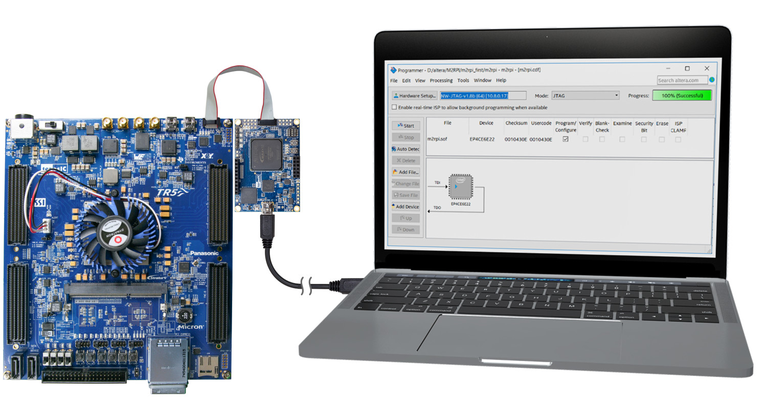
USB-Blaster II Download Cable
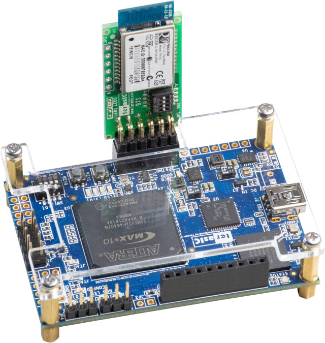
Connect BTS-TMD
Connect WS2812B LED Strip