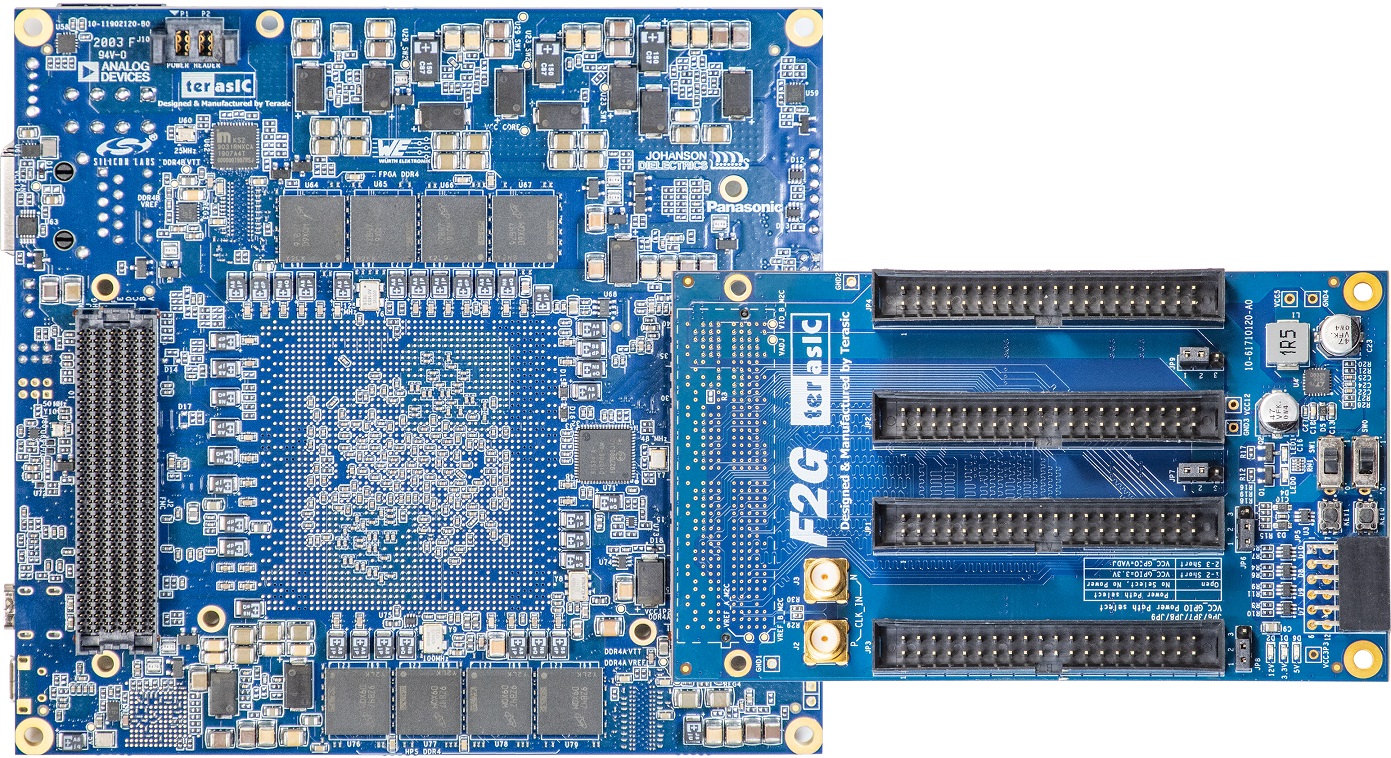
FPGA
- Intel Stratix 10 Soc FPGA 1SX280HU2F50E1VG
FPGA Configuration
- On-Board USB Blaster II for FPGA programming and Debug
- AS Mode configuration from QSPI Flash
Clock and User Interface
- Four 50Mhz Single-ended Clock Source
- One 100Mhz Single-ended Clock Source
- Clock Generator Si5341
- LED x2, Button x2, Dip Switch x2, CPU Reset
- Power Switch
- FMC Adjustable Voltage 1.8V/1.5V/1.2V
- FMC+ Adjustable Voltage 1.8V/1.5V/1.2V
Memory
- 1024Mbit QSPI Flash (EPCQL1024 Compliant)
- Total of 64GB DDR4 x72 2133MT/s with ECC
- Two independent DDR4 banks
- One bank is shared with FPGA and HPS
Communication and Expansion
- FMC (Vita57.1) connector with 10 transceivers
- FMC+(Vita57.4) connector with 24 transceivers
HPS
- MicroSD Socket
- Gigabit Ethernet with RJ45
- USB OTG with Micro USB Connector
- UART to USB with Mini USB Connector
- RTC
- LED x1, Button x1, Cold Reset Button
- 1x6 GPIO Header
Dashboard System
- Input Power Monitor
- FPGA and Board Temperature Monitor
- Fan Control and Monitor
- Auto Fan Speed
- Auto Shutdown
Power Source
- 12V from 2x4 PCIe connector
- 12V from Samtec connector (reserved for carrier board)
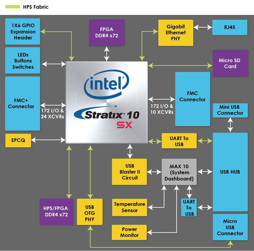
Block Diagram
Apollo Developer Kit
- The Kit is composed by
- Apollo S10 Module (heatsink installed)
- Apollo Carrier Board
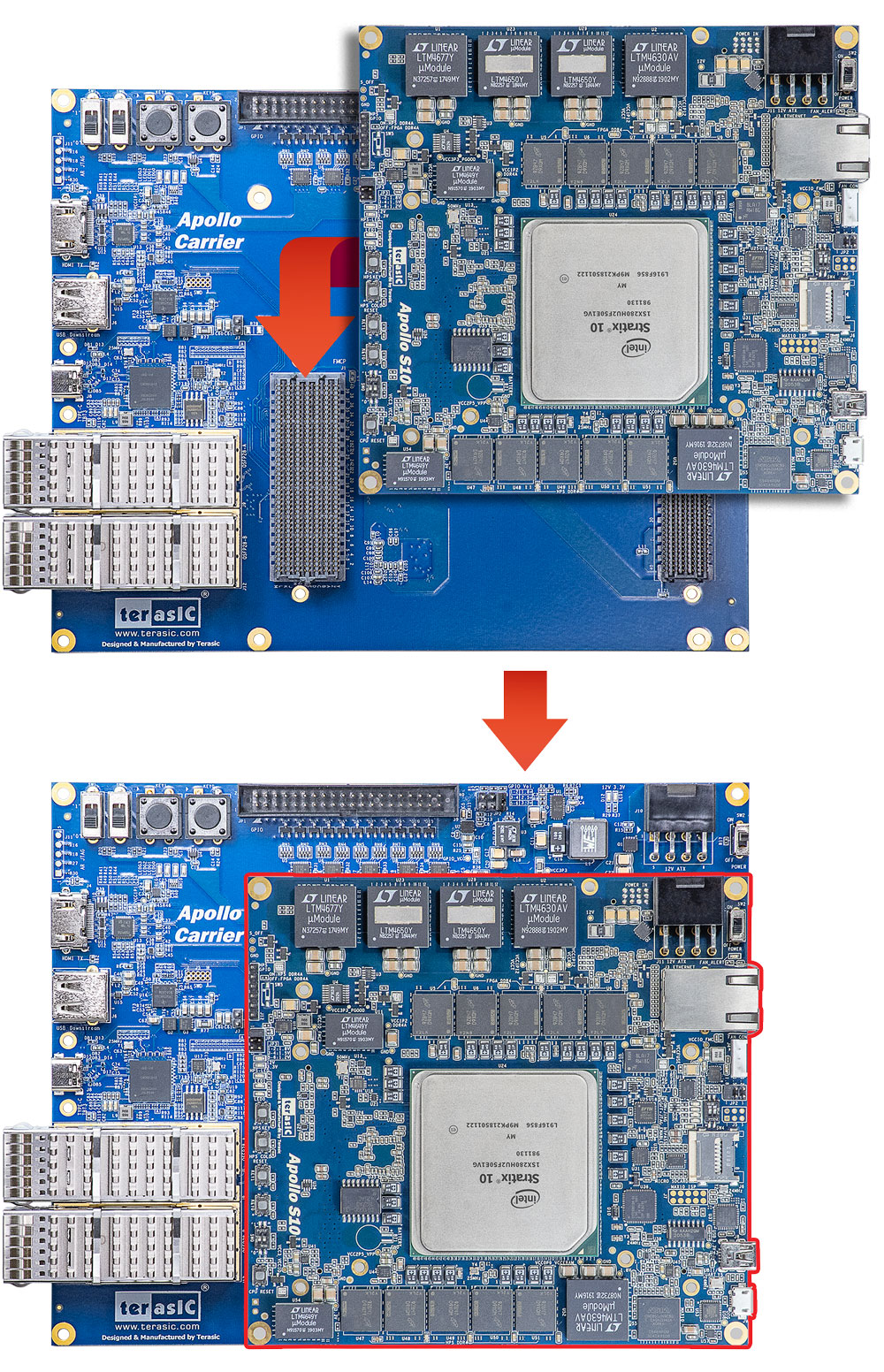
- The Apollo Carrier Board features includes:
- PCIe Gen3 x4 via Thunderbolt 3 (Type-C Connector)
- USB Downstream port via Thunderbolt 3 (Type-A Connector)
- Two QSFP connectors (40G Ethernet)
- Clock Generator to provide reference clock for transceiver IP
- LED x4, Button x2, Switch x2
- 2x20 GPIO Expansion Header. Adjustable IO Standard 3.3V/2.5V/1.8V.
- HDMI TX port (Rev.C or later version supported)
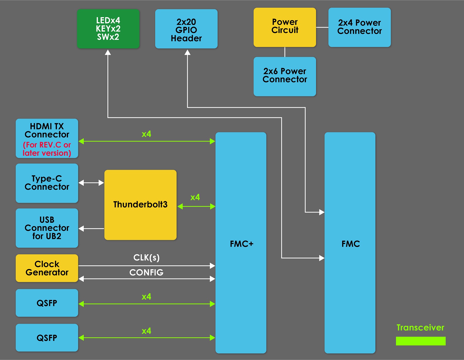
- The Block Diagram of Apollo Carrier Board
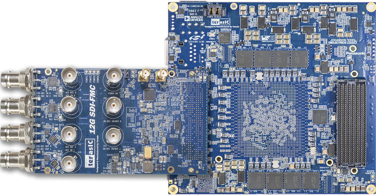
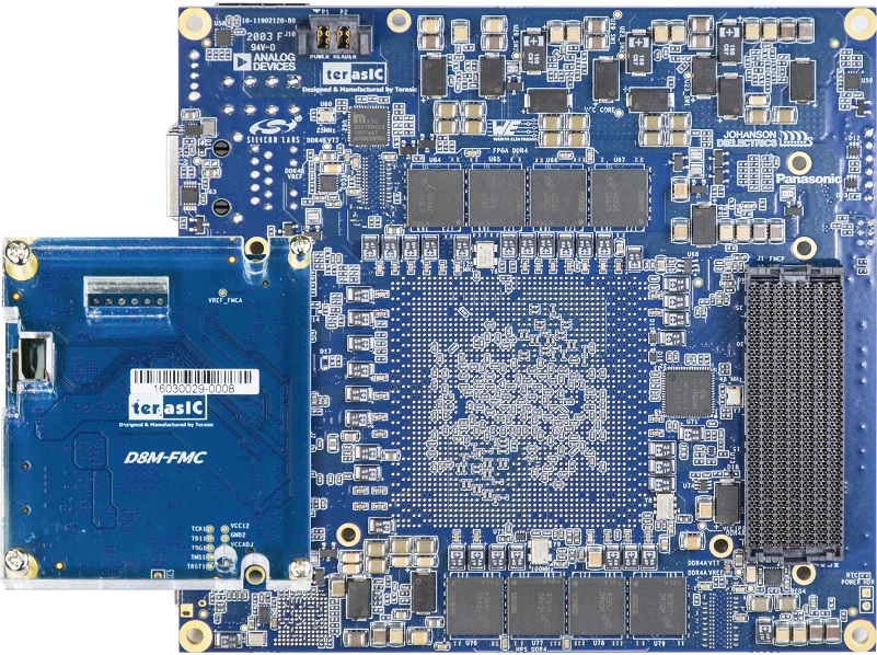
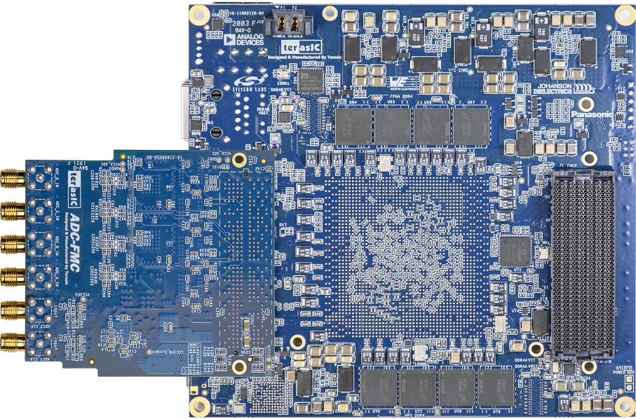
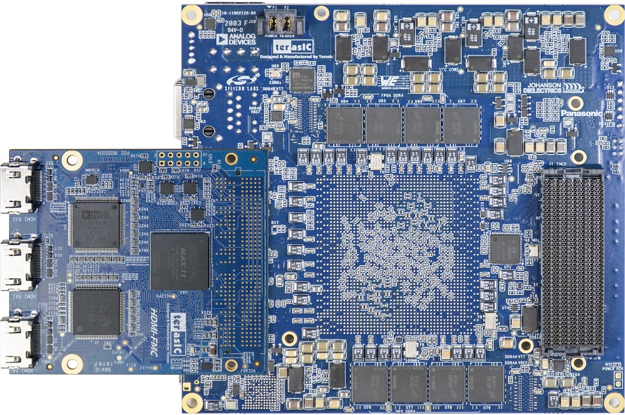
Connection to FMC Daughter Card:
- Connect to 12G SDI-FMC Daughter Card:
- Connect to D8M-FMC Daughter Card:
- Connect to ADC-FMC Daughter Card:
- Connect to HDMI-FMC Daughter Card:
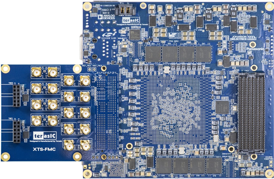
- Connect to XTS-FMC Daughter Card:
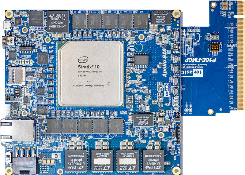
- Connect to P16E-FMCP Daughter Card:
- Connect to F2G-FMC Daughter Card:
